Diode Circuits Set 1
[1991 : 2 M] Figure shows an electronic voltage regulator. The zener diode may be assumed to require a minimum current of 25 mA for satisfactory operations. The value of R required for satisfactory voltage regulation of the circuit is
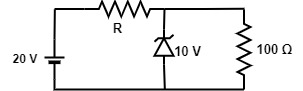
Ans: 80 Ω
Explanation:- Let us calculate the current in 100 Ω resistance and in the resistance R,
Current in 100 Ω resistance
I_{100}=\frac{10V}{100\Omega}=100\;mAI2 = 25 mA
Current in resistance R, = 100 mA + 25 mA
= 125 mA
Also, 20 – 10 = 125 x 10-3 x R
R=\frac{10\times1000}{125}=80\OmegaThe correct answer is 80 Ω.
[1996 : 1 M] The depletion region (or) space charge region (or) transition region in a semiconductor p-n junction diode has
(a) electrons and holes
(b) positive ions and electrons
(c) positive and negative ions
(d) negative ions and holes
Ans: (c)
Explanation:- Depletion region is a space-charge region in p-n junction diode.
Therefore the Charge recombination occurs in depletion region.
So, option (c) is the correct answer.
[1999 : 1 M] As temperature is increased, the voltage across a diode carrying a constant current
(a) increases
(b) decreases
(c) remains constant
(d) may increase or decrease depending upon the doping levels in the junction
Ans: (b)
Explanation When the temperature is increased, there is increase in temperature results in generation of more charge carriers or electron hole pairs which are responsible for an increase in the current flowing through the diode.
\frac{dV_D}{dT}=-2.5mV/^oCSo, option (b) is the correct answer.
[1999 : 1 M] The mobility of an electron in a conductor expressed in terms of
(a) cm2/V-sec
(b) cm/V-sec
(c) cm2/V
(d) cm2/Sec
Ans: (a)
Explanation The measurement of how fast an electron can move through a semiconductor or a metal which is under the influence of an external electric field. Therefore, it is expressed in terms of cm2/V-sec
\mu=\frac{Drift\;velocity}{Electric\;field}Therefore, option (a) is the correct answer.
[2000 : 2 M] A diode whose terminal characteristics are related as i_D=I_se^{V/V_T}, where Is is the reverse saturation current and VT is thermal voltage (= 25 mV), is biased at iD = 2 mA. Its dynamic resistance is
(a) 25 Ω
(b) 12.5 Ω
(c) 50 Ω
(d) 100 Ω
Ans: (b)
Explanation:- We know that the dynamic resistance is defined from the I-V characteristics of a diode in forward biased.
Given that , VT= 25 mV , iD= 2 mA
r_D=\frac{V_T}{I_D}=\frac{25\;mV}{2\;mA}=12.5\;\OmegaSo, option (b) is the correct answer.
[2002 : 1 M] The forward resistance of the diode shown in figure is 5 Ω and the remaining parameters are same as those of ideal diode. The DC components of the source current is
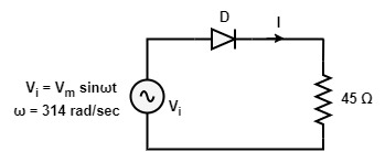
(a) \frac{V_m}{50\pi}
(b) \frac{V_m}{50\pi\sqrt2}
(c) \frac{V_m}{100\pi\sqrt2}
(d) \frac{2V_m}{50\pi\sqrt2}
Ans: (a)
Explanation:- The average voltage is given by,
V_{av}=\frac{V_m}\piThe average current is given by,
I_{av}=\frac{V_{av}}R=\frac{V_{av}}{\left(5+45\right)}=\frac{V_{av}}{50} =\frac{V_m}{50\pi}Therefore, option (a) is the correct answer.
[2002 : 1 M] The cut-in voltage of both zener diode Dz and D shown in figure is 0.7 V, while breakdown voltage of the zener is 3.3 V and reverse break down of D is 5 V. The other parameters can be assumed to be the same as those of an ideal diode. The values of the peak output voltage (V0) are
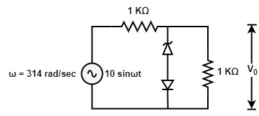
(a) 3.3 V in the positive half cycle and 1.4 V in the negative half cycle.
(b) 4 V in the positive half cycle and 5 V in the negative half cycle.
(c) 3.3 V in the both positive and negative half cycle.
(d) 4 V in the both positive and negative half cycle.
Ans: (b)
Explanation:- Let us assume two cases,
Case-I :- For positive half cycle, at peak input voltage
So, Vo = 4 V
Case-II :- For negative half cycle, at peak input voltage
So, V_o=10\times\left(\frac1{1+1}\right)=5V
So, option (b) is the correct answer.
[2002 : 2 M] In the single-phase diode bridge rectifier shown in figure, the load resistor is R = 50 Ω. The source voltage is V = 200 sin ωt, where ω = 2π x 50 rad/s. The power dissipated in the load R is
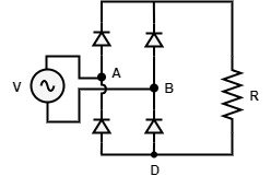
(a) \frac{3200}\pi W
(b) 400 W
(c) \frac{400}\pi W
(d) 800 W
Ans: (b)
Explanation:- The rms voltage is given as,
V_{rms}=\frac{V_m}{\sqrt2} P=\frac{V_{rms}^2}R=\frac{V_m^2}{2R} =\frac{200^2}{2\times50}=400WSo, option (b) is the correct answer.
[2003 : 2 M] A voltage signal 10 sin ωt is applied to the circuit with ideal diodes, as shown in figure. The maximum, and minimum values of the output waveform Vout of the circuit are respectively.
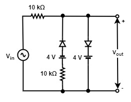
(a) + 10 V and – 10 V
(b) + 4 V and – 4 V
(c) + 7 V and – 4 V
(d) + 4 V and – 7 V
Ans: (d)
Explanation:- Let us consider two cases,
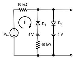
Case-I :- For +ve cycle, when Vin< -4 V
(Vin> 4 V) D2 ON, D1 OFF, Vout =4 V
where Vin < 4 V, then Vout = Vin because D2 also become (OFF).
Case-II :- For -ve cycle, when Vin < -4
D1 ON, D2 OFF
I=\frac{V_{in}+4}{20k}but, Vin = -ve
∴ I=\frac{-V_{in}+4}{20}=\frac{-3}{10}mA
(∵ for minimum output Vin = -10 V)
V_o=\frac{-3}{10}\times10k-4=-7VSo, option (d) is the correct answer.
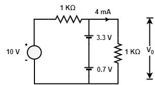
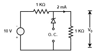
[2004 : 1 M] The current through the Zener diode in figure is
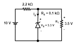
(a) 33 mA
(b) 3.3 mA
(c) 2 mA
(d) 0 mA
Ans: (c)
Explanation:- Given that , Rz= 0.1 kΩ , Vz= 3.3 V
The current in the zener diode is calculated as,
R_Z=\frac{\triangle V_z}{\triangle I_z}=\frac{3.5-3.3}{\triangle I_z}∴ \triangle I_z=\frac{0.2}{0.1k}=2\;mA
So, option (c) is the correct answer.